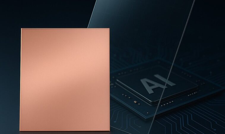
Remember CIT (Copper Innovation Technology)? Last summer, we introduced you to this scrappy South Korean innovator and their game-changing recycled copper antennas. Now they’re tackling something even bolder – reimagining how AI chips get built.
Meet CuFlat-PKGCore™, their latest brainchild that transforms the atomic sputtering magic behind those flexible antennas into something completely different: creating impossibly flat copper surfaces on glass for next-generation semiconductors.
Every computer you’ve opened reveals those familiar green circuit boards made from FR4 material – the reliable workhorse that’s carried us through decades of computing. But here’s the problem: AI is writing checks that FR4 simply can’t cash.
“We’re witnessing a fundamental mismatch,” explains Dr. Sarah Chen, a semiconductor analyst tracking this challenge. “Traditional substrates are gasping under AI’s relentless demands. When milliseconds determine whether your AI query succeeds or fails, every component becomes critical.”
This is where CIT’s engineers had their eureka moment. Why not replace those aging substrates with ultra-flat copper deposited directly on glass? Simple concept, revolutionary execution.
The secret lies in their Atomic Sputtering Epitaxy process – the same technology powering their antenna breakthrough, but now laser-focused on precision rather than flexibility. Instead of messy chemical baths requiring multiple steps, ASE works like a molecular printer, depositing copper atoms at a modest 212°F.
The results border on miraculous: copper surfaces with roughness measuring less than 4 nanometers. If a human hair were the width of a highway, this surface would have bumps smaller than pebbles.
“When we first achieved these smoothness levels, our team thought the measurement equipment was broken,” admits CIT’s lead engineer. “We ran the tests five times before believing our own data.”
This obsessive smoothness enables circuit connections so precise they make current technology look crude. Signal integrity improves dramatically, and heat management becomes far more efficient.
But CIT hasn’t abandoned their environmental principles while chasing performance. CuFlat-PKGCore™ maintains their commitment to 100% recycled copper while eliminating wet chemicals entirely. No wastewater, no toxic runoff, and a carbon footprint slashed by over 95% – from 3.75 tons down to 0.00175 tons per unit.
CIT isn’t operating in a vacuum. Tech giants Intel and Samsung are pouring resources into glass substrate research, with commercial launches planned for 2025-2026. The industry recognizes what’s coming: glass substrates that expand in harmony with silicon chips, eliminating heat-induced warping while packing more computational power into smaller spaces.
What captivates me most is watching CIT pivot their core innovation across different markets. The same atomic precision handling 100GHz mmWave signals in their antennas now crafts the intricate pathways AI chips depend on. Their antenna division targets expanding 5G markets, while CuFlat-PKGCore™ plants their flag in AI’s explosive growth.
Let’s strip away the jargon for a moment. Every time you ask ChatGPT a complex question, generate an AI image, or use your phone’s smart features, you’re bumping against limitations built into current chip packaging. These aren’t software problems–they’re physical constraints no amount of clever coding can overcome.
Technologies like CuFlat-PKGCore™ don’t just incrementally improve performance; they shatter existing bottlenecks entirely. We’re talking about AI systems processing information faster while consuming less energy–the holy grail of sustainable computing.
The semiconductor packaging materials market is racing toward $50 billion by 2025. As AI applications multiply exponentially, companies eliminating fundamental performance barriers will capture disproportionate value.
The real test lies ahead: scaling laboratory brilliance to industrial manufacturing. The semiconductor industry demands perfection measured in parts per billion. Yet with Intel and Samsung already committing billions to glass substrate futures, the industry’s direction seems inevitable.
Next time AI capabilities leave you speechless, remember the invisible revolution happening at the atomic level. While everyone focuses on algorithms, companies like CIT are rewriting the fundamental rules of what’s physically possible. Their journey from flexible antennas to AI chip foundations shows that sometimes the biggest breakthroughs come from applying existing excellence to entirely new problems.
This story has been brought to you in partnership with AVING News Network.


